NetFPGA-SUME资源对比
introduction
本帖主要介绍NetFPGA-SUME板上资源介绍。
NetFPGA-SUME开发板FPGA芯片型号xc7vx690tffg1761-3。

芯片资源
我们将NetFPGA-SUME的芯片xc7vx690t 与 XCKU060 做对比。
| 芯片型号 | Logic cells | CLB Flip-Flops | DSP slices | Max. Distributed RAM (Kb) | BRAM(kb) |
|---|---|---|---|---|---|
| XC7VX690T | 693120 | 866400 | 3600 | 10888 | 52920 |
| XCKU060 | 726000 | 663360 | 2760 | 9180 | 38000 |
Memory
主要包括DRAM和SRAM:
- Two 4GB DDR3 SODIMMs (MT8KTF51264Hz- 1G9E1)
- 64 bit wide buses clocked at 850 MHz (1700 MT/s)
- Three 72Mbit QDRII+ SRAMs (CY7C25652KV18-500BZXC)
- 36 bit wide buses clocked at 500 MHz (1000 MT/s)
DSP
DSP基本架构如下: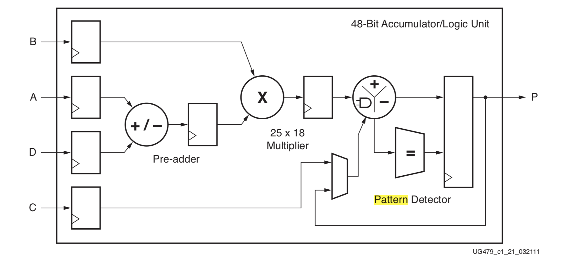 Some highlights of the DSP functionality include:
- 25 × 18 two’s-complement multiplier:
- Dynamic bypass
- 48-bit accumulator:
- Can be used as a synchronous up/down counter
- Power saving pre-adder:
- Optimizes symmetrical filter applications and reduces DSP slice requirements
- Single-instruction-multiple-data (SIMD) arithmetic unit:
- Dual 24-bit or quad 12-bit add/subtract/accumulate
- Optional logic unit:
- Can generate any one of ten different logic functions of the two operands
- Pattern detector:
- Convergent or symmetric rounding
- 96-bit-wide logic functions when used in conjunction with the logic unit
- Advanced features:
- Optional pipelining and dedicated buses for cascading
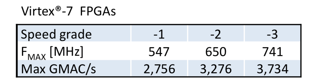
DSP可运行的最大频率如下图所示: